Im Develops Computer on Glass
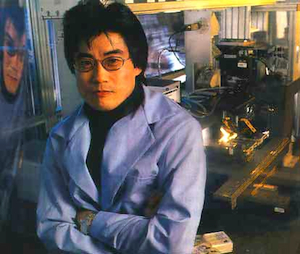 Photo: James Im, in his laboratory on the 11th floor of the Mudd building, sits in front of the laser system where his patented process can convert poor quality silicon on glass to the ideal single crystal structure for transistors and solar cells.
James Im's smile is so warm it could melt ice, an ironic coincidence since he loves to study how things melt and freeze. He studies thin films and his hope is to put a computer on a transparency. This young scientist with an impish grin and a sense of humor to match calls his research "beating silicon with silicon" or, translated into more pedestrian terms, putting silicon-based transistors on inexpensive and transparent glass (SiO2) or plastic substrates and not on Si wafers as has been done previously.
The unpretentious graduate of MIT and Cornell and associate professor of materials science and engineering has developed a laser-based process that will revolutionize semiconductor manufacture and flat panel displays. His new method is called "SLS," sequential lateral solidification, and the fundamental breakthrough he discovered is that it is how a substance is melted and solidified that makes the difference.
Dr. Im was not the first to use lasers in the search to find a way to create high quality crystalline structures with nicely arranged Si atoms. Many previous researchers tried, but found that their results were not good enough. Eight years ago, Dr. Im and his graduate students began their own work with lasers, initially focusing on finding out what was taking place and then coming up with a way to do things differently. While others used uniform laser light to flood-irradiate a film, he theorized that he could shape the excimer laser light into thousands of extremely small beamlets. Using these tiny beamlets to control melting and solidification of the films, he was able to induce the illusive, perfect crystalline structure of silicon.
"By using a short pulse-duration laser to zap the film, you can improve the material by extreme melting and solidifying. It's very, very, very quick," explains Im. The rearranged silicon atoms of a single crystal film can then be used to create a variety of devices, from solar cells to thin-film transistors for flat panel displays for computers, on glass or on plastic sheets. "With this technology," he said, "it is possible to think about putting an entire computer on a sheet of glass or plastic. It's just a matter of time."
"Like alchemists, we materials engineers take a bad material and make it good," Im said. His present laboratory, on the 11th floor of the Mudd building, is the fourth iteration of labs. It has been built with lasers, optics, mirrors and lenses that are put together to manipulate the melting and freezing of thin films. The sample sits on a translator, which sits on a 4,000-pound solid granite table, the maximum weight allowed in the building's freight elevator. Im jokes that the table was moved into his lab by the same power that built the pyramids in Egypt and the Great Wall of China: "lots of students."
Once the granite-based system was in place, Im's research team began another round of experiments. "What we do is like melting stone on butter," he said. "We put together our equipment in such a way that it permits us to manipulate the rapid melting and freezing of thin films within an extremely short time period," he said. "We melt and solidify silicon on glass, which melts at a low temperature, like the butter. By controlling the transformations, we can consistently get nicely arranged atoms to make a perfect crystalline structure. It provides the ultimate semiconductor material, a single-crystal Si," he said.
This process will initiate a new field of low-temperature, single-crystal-based thin-film transistors that can be used for active-matrix liquid crystal displays, active matrix organic electroluminescent displays, silicon-on-insulator substrates, three-dimensional integrated circuits, and computer-on-glass/plastic products. Dr. Im's development of sequential lateral solidification has produced an excited reaction among the research and business communities both here and abroad. Columbia's Science and Technology Ventures (STV) has helped Dr. Im translate his research into non-exclusive contracts with manufacturers who are retooling their factories to accommodate the new technology.
"James has made a fundamental breakthrough that has led to improved semiconductor substrates," said Dr. Frank J. Carrigan, STV's Director of Technology Commercialization. "Lots of people have tried to do this and James has found a way. It solves the problems and will create a better product. In short, it's a '10;' it's the killer app." More than 40% of the display industry already has licensed his new technology. Having found the way to produce the perfect silicon crystal, Dr. Im and his researchers have now turned their attention to improving the copper wiring used in chips for integrated circuits. By rearranging the microstructure of the copper interconnects, he can potentially all but eliminate the problem of electromigration failure.
"This method of zapping copper can solve the bottleneck in performance by making copper wires more conductive and failure-proof," said Dr. Im. "By doing so, it indirectly allows Moore's Law [that each new generation of microchip will be significantly better than the previous one] to continue to hold true." This breakthrough will be presented at a conference of the Materials Research Society in mid-April. "I tell my graduate students that they need to find the right balance between pure science research and concerns with its technological relevance," said Dr. Im, "but, of course, I'm still struggling to find the balance myself."