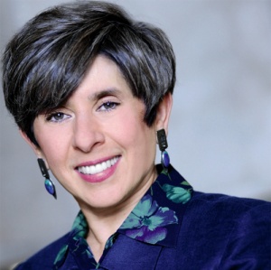
Katayun Barmak: Philips Electronics Professor
 Dr. Katayun Barmak joins the APAM Department as the new Philips Electronics Professor.
The Philips Electronics Professorship endowment was established by Philips, the international electronics company headquartered in The Netherlands, in the Deparmtent of Applied Physics and Applied Mathematics to honor the late Professor Gertrude Neumark Rothschild, Howe Professor Emerita of Materials Science and Engineering, for her pioneering role as a woman engineer. Dr. Neumark, who was employed by Philips Laboratory for 25 years, was on of the world’s foremost experts on doping wide band-gap semiconductors and held a number of patents on wide band-gap semiconductor technology.
Dr. Barmak obtained her B.A. (First Class Hons.) and M.A. degrees in Natural Sciences, Metallurgy and Materials Science from the University of Cambridge, England in 1983 and 1987, respectively. She completed her M.S. in Metallurgy and Ph.D. in Materials Science at the Massachusetts Institute of Technology in 1985 and 1989, respectively. During her doctoral work she was a recipient of an AT&T Foundation Fellowship. Prior to her appointment to the Faculty at Lehigh in 1992, Dr. Barmak spent three years at IBM T.J. Watson Research Center and IBM East Fishkill development laboratory working on materials, structures and processes for advanced generations of field effect and bipolar junction transistors. She joined the Department of Materials Science and Engineering at Carnegie Mellon University in 1999 and was promoted to the rank of Full Professor in 2002. Dr. Barmak received the National Young Investigator in 1994 and a Deutscheforschunggemeinschaft Fellowship the same year. She was one of four Technical Chairs of the Materials Research Society Meeting in Spring 1999. She was a Visiting Scientist at the IBM T. J. Watson Research Center 1998-2004. She is an Associate Editor of the Journal of Electronic Materials.
Her research interests include processing, properties, crystal structure, grain structure, and texture of polycrystalline metal films for application in integrated circuits and magnetic recording media; thermodynamics and kinetics of reactions and phase transformations in nanostructured films; experimental, analytical and simulational studies of transformations and associated microstructures in thin films; and properties of grain boundaries. Characterization techniques of interest include differential scanning calorimetry (DSC), x-ray and electron diffraction (XRD, ED), and transmission, scanning and orientation imaging microscopy (TEM, SEM, OIM).
Related Article
